
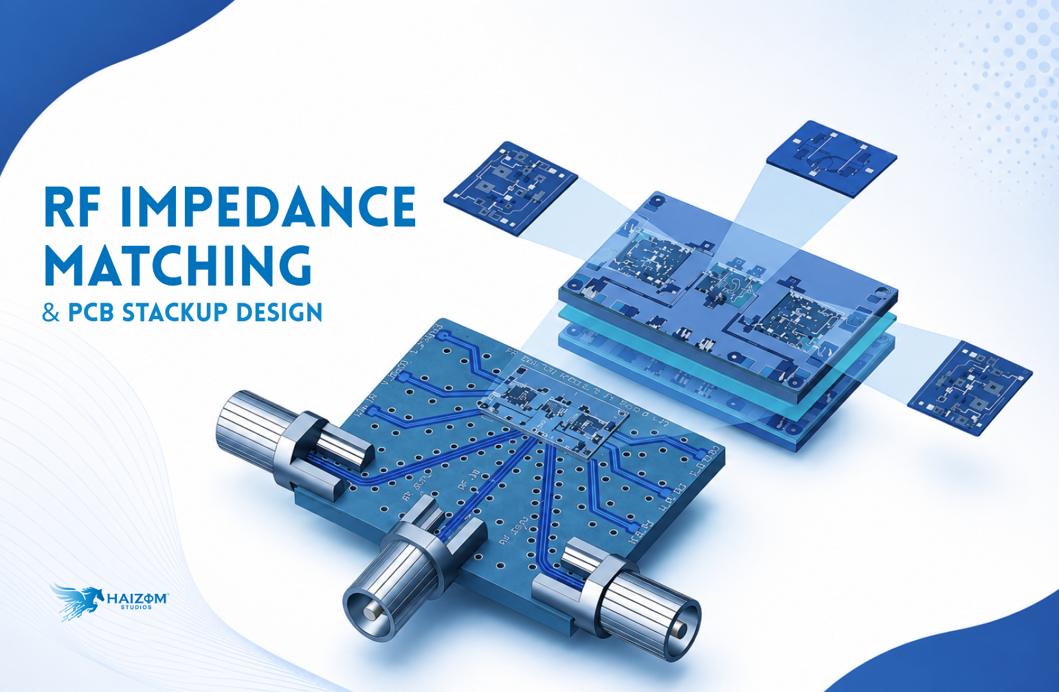

RF Impedance Matching & PCB Stackup Design
Modern RF systems rely heavily on precise impedance matching and optimized PCB stackup design to maintain signal integrity across high-frequency communication channels.
Why 50 Ω Controlled Impedance Matters
In RF PCB design, maintaining 50 Ω controlled impedance ensures efficient power transfer between the cellular module and antenna system while minimizing signal reflections and transmission loss.
Key Benefits
- Improved RF signal integrity
- Reduced EMI and signal distortion
- Better LTE/GNSS/Wi-Fi performance
- Stable high-frequency communication
PCB Stackup Visualization
The illustration highlights a multilayer RF PCB featuring:
- Controlled impedance transmission lines
- Dedicated ground planes
- Cellular module connected to a U.FL antenna connector
- Cutaway multilayer PCB stackup view
- Smooth RF signal propagation
Layer Structure
- RF Signal Layer
- Ground Plane
- Power Plane
- Signal Routing Layer
Matched vs Mismatched Impedance
Matched Impedance
✔ Smooth signal flow
✔ Minimal reflections
✔ Clean waveform transmission
Mismatched Impedance
✖ Signal reflections
✖ Distorted RF waves
✖ Reduced communication efficiency
Featured Engineering Elements
- 50 Ω Controlled Impedance
- RF Signal Integrity
- PCB Stackup
- Ground Plane
- LTE / GNSS / Wi-Fi wireless signal visualization
#RFDesign #PCBDesign #SignalIntegrity #ImpedanceMatching #ElectronicsEngineering #RFEngineering #PCBStackup #WirelessCommunication #Semiconductor #EmbeddedSystems